 LAMP·Lab
IIT Bombay
LAMP·Lab
IIT Bombay
LAMP·Lab
IIT Bombay
LAMP·Lab
IIT Bombay
Translating cutting-edge laser research into practical industrial applications.
The LAMP Laboratory offers various engagement models for industry partners to access our expertise, facilities, and research capabilities. We are committed to translating cutting-edge research into practical industrial applications.
Gain access to our state-of-the-art labs and laser systems for testing, prototyping, and collaborative innovation.
Partner with our faculty and researchers on cutting-edge R&D initiatives aligned with your organization’s goals.
Leverage our domain knowledge and problem-solving expertise to address specific technical or strategic challenges.
Discover the wide range of capabilities and expertise available at the LAMP laboratory. All samples below were processed in-house.
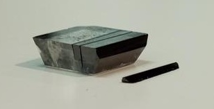
High-precision laser cutting of diamonds and difficult-to-cut materials.

High-precision micro-drilling on metal plates up to a few mm thick.

Glass–glass welding using aluminium filler with encapsulated solar cell.

High-precision complex shape cutting on polymer samples.

A butterfly pattern with various colours produced on a stainless steel sample.

Ablation of an 80 nm SiNx film on Si for PERC solar cell application.

Surface textures of micron and sub-micron features produced on a Si sample.

Laser-induced periodic surface structures produced on a diamond sample.

Precision cutting of a 5 mm thick glass with no damage.

Creating complex art inside a glass sample.

Image of a lion produced on a glass sample.

Microchannels produced on a glass sample for microfluidic applications.
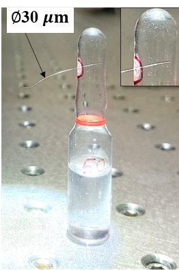
Arrays of micro-vias drilled through ampoule walls for precision dosing.
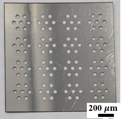
Dense arrays of through micro-holes drilled with high positional accuracy.
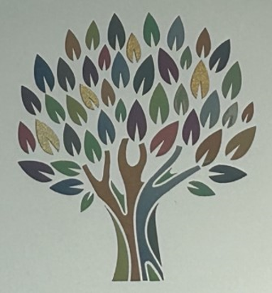
Vivid, permanent colour marking on stainless steel via controlled surface oxidation.
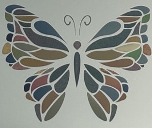
Multi-colour laser marking on stainless steel with no inks or coatings.
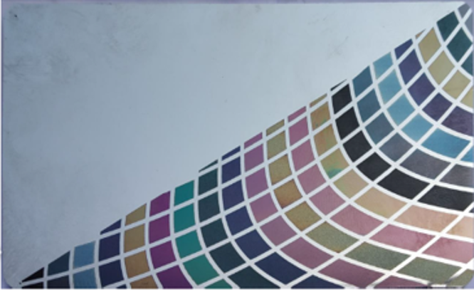
High-resolution colour images produced directly on stainless steel.
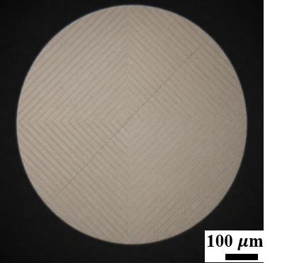
Precise periodic gratings machined on single-crystal diamond.
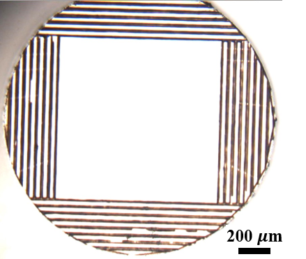
High-fidelity diffraction gratings fabricated on diamond surfaces.
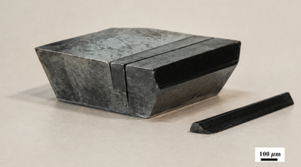
Clean, crack-free cutting of diamond, one of the hardest materials.
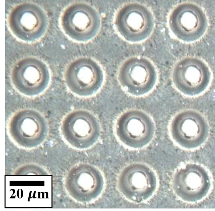
Ordered micro-dimple arrays for friction and lubrication control.
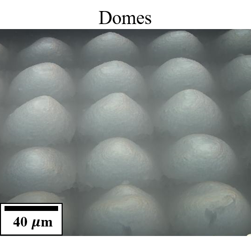
Raised micro-dome structures for optical and wetting applications.
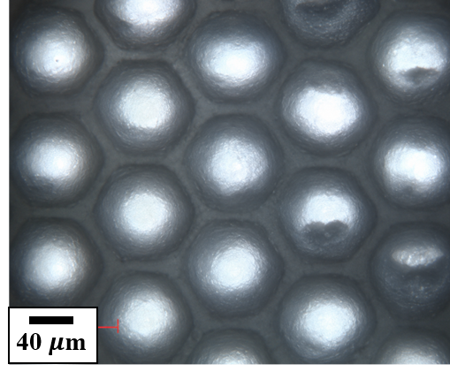
Hexagonal micro-textures patterned uniformly over large areas.
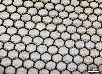
Honeycomb lattices machined with sharp, uniform cell walls.
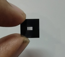
Fine-feature cutting of thin masks for microfabrication.
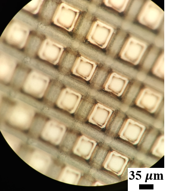
High-aspect-ratio micro-pillars fabricated on diamond.

Through micro-holes of ~40 µm diameter drilled in glass without cracking.
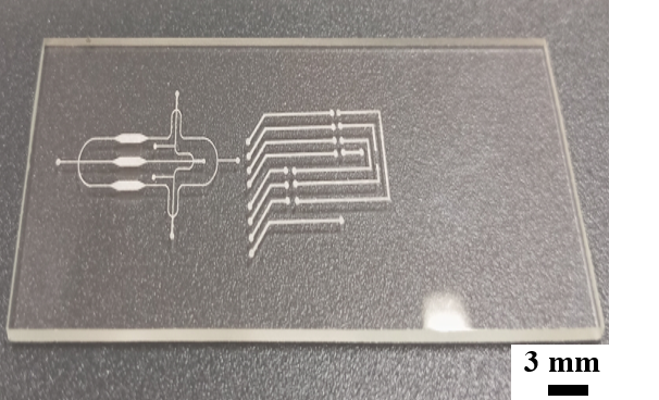
Smooth microchannels for microfluidic and lab-on-chip devices.
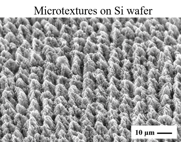
Controlled micro-textures across silicon wafers for photovoltaics.
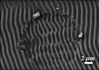
Sub-micron surface textures produced on diamond.
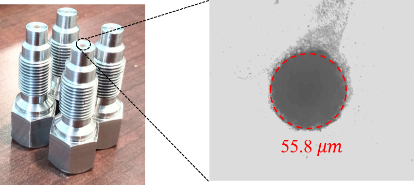
Precision micro-holes drilled in nozzle components for fluid control.
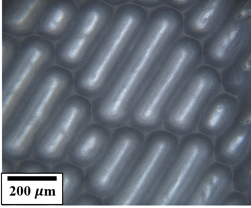
Bio-inspired sharklet patterns for anti-fouling surfaces.
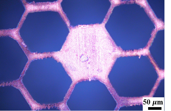
Delicate spider-web patterns cut with high precision.
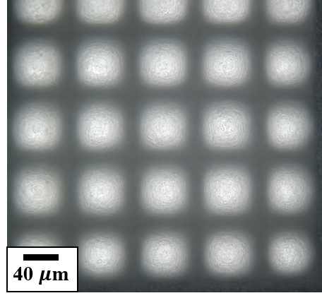
Regular square micro-texture arrays for surface engineering.
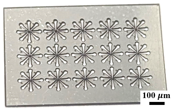
Sharp-cornered star shapes cut cleanly from thin sheets.
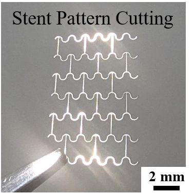
Fine strut patterns cut for cardiovascular stents.
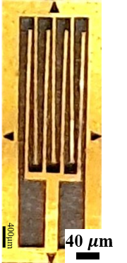
Fine conductive strain-gauge patterns fabricated by laser.
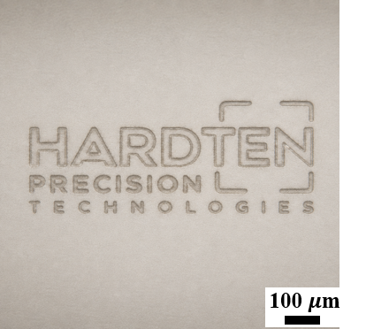
Logos marked beneath the surface of diamond without surface damage.

Crisp logos marked directly on diamond surfaces.
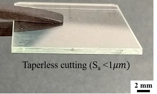
Straight-walled, taper-free cutting through thick sections.
Our research relies heavily on multiphysics computational modelling. Here are some of our process simulations.

Molecular dynamics simulation of ultrafast laser–matter interaction.

Computer simulation of high-aspect-ratio laser drilling.

FE simulation of laser directed energy deposition with in-situ rolling.

FE-based thermo-mechanical simulation of laser-assisted machining.
Partner with the LAMP Laboratory for access to cutting-edge laser technology, expert knowledge, and collaborative research opportunities.
Contact our team